
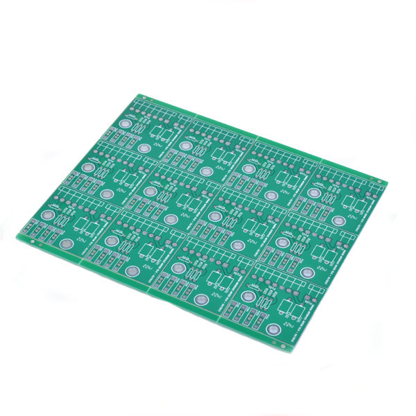
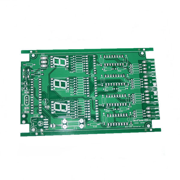
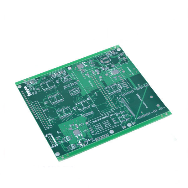
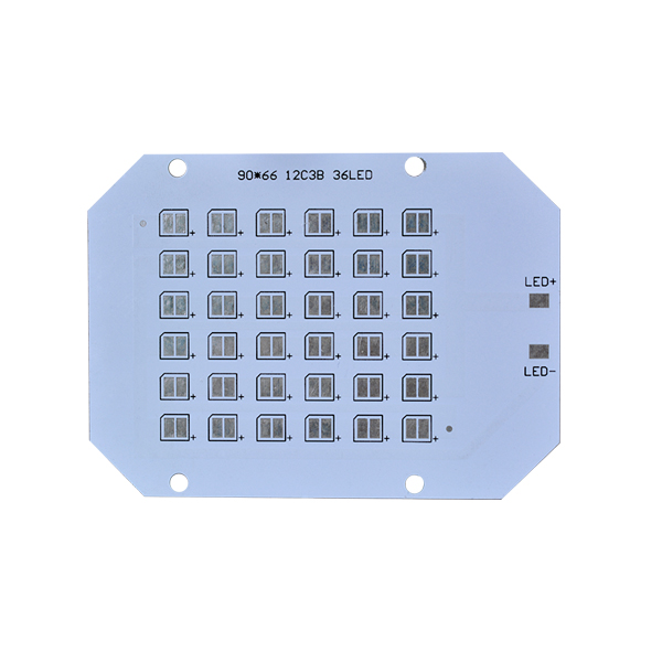
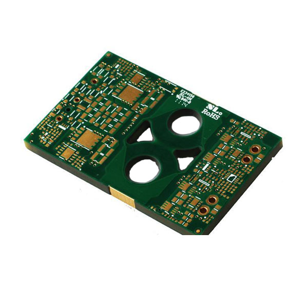
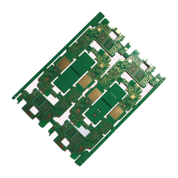
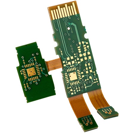
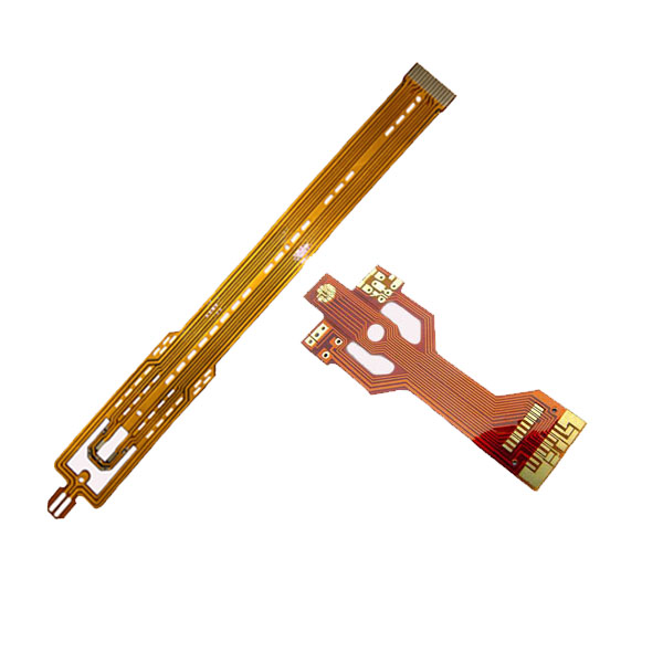
ייצור PCB
PCB Fabrication is one of our primary services, which is also known as PCB Manufacturing, PCB Printing Service. All our services are under NDA(הסכם סודיות) Protection which makes you stay away from intellectual property concern. Below are the PCB types we manufacture.
זמן אספקה(Days)
| צד בודד/כפול | 4 שִׁכבָה | 6 שִׁכבָה | over 8 שִׁכבָה | HDI | |
| זמן אספקה לדוגמא(נוֹרמָלִי) | 5-6 | 6-7 | 7-8 | 10-12 | 15-20 |
| זמן אספקה לדוגמא(הכי מהיר) | 48-72 שעות | 5 | 6 | 6-7 | 12 |
| זמן אספקת ייצור המוני(אצווה ראשונה) | 7-9 | 10-12 | 13-15 | 16 | 20 |
PCB Fabrication Capability
| PCB Fabrication Capability | ||
| No | פָּרִיט | PCB Process Capability |
| 1 | base material | Normal TG FR4, High TG FR4, PTFE, רוג'רס, Low Dk/Df etc. |
| 2 | צבע מסכת הלחמה | green, אָדוֹם, כְּחוֹל, לָבָן, צָהוֹב, purple,שָׁחוֹר |
| 3 | Legend color | לָבָן, צָהוֹב, שָׁחוֹר, אָדוֹם |
| 4 | Surface treatment type | לְהַסכִּים, Immersion tin, HAF, HAF LF, OSP, flash gold, gold finger, sterling silver |
| 5 | Max. layer-up(L) | 50 |
| 6 | Max. unit size (מ"מ) | 620*813 (24″*32″) |
| 7 | Max. working panel size (מ"מ) | 620*900 (24″x35.4″) |
| 8 | Max. עובי לוח (מ"מ) | 12 |
| 9 | לי. עובי לוח(מ"מ) | 0.3 |
| 10 | סובלנות לעובי לוח (מ"מ) | T<1.0 מ"מ: +/-0.10מ"מ ; T≥1.00mm: +/-10% |
| 11 | Registration tolerance (מ"מ) | +/-0.10 |
| 12 | לי. mechanical drilling hole diameter (מ"מ) | 0.15 |
| 13 | לי. laser drilling hole diameter(מ"מ) | 0.075 |
| 14 | Max. aspect(through hole) | 15:1 |
| Max. aspect(micro-via) | 1.3:1 | |
| 15 | לי. hole edge to copper space(מ"מ) | L≤10, 0.15;L=12-22,0.175;L=24-34, 0.2;L=36-44, 0.25;L>44, 0.3 |
| 16 | לי. Inner layer clearance(מ"מ) | 0.15 |
| 17 | לי. hole edge to hole edge space(מ"מ) | 0.28 |
| 18 | לי. hole edge to profile line space(מ"מ) | 0.2 |
| 19 | לי. Inner layer copper to profile line space (מ"מ) | 0.2 |
| 20 | Registration tolerance between holes (מ"מ) | ±0.05 |
| 21 | Max. finished copper thickness(אֶחָד) | Outer Layer: 420 (12עוז) Inner Layer: 210 (6עוז) |
| 22 | לי. trace width (מ"מ) | 0.075 (3מִיל) |
| 23 | לי. trace space (מ"מ) | 0.075 (3מִיל) |
| 24 | Solder mask thickness (אֶחָד) | line corner: >8 (0.3מִיל) upon copper: >10 (0.4מִיל) |
| 25 | ENIG golden thickness (אֶחָד) | 0.025-0.125 |
| 26 | ENIG nickle thickness (אֶחָד) | 3-9 |
| 27 | Sterling silver thickness (אֶחָד) | 0.15-0.75 |
| 28 | לי. HAL tin thickness (אֶחָד) | 0.75 |
| 29 | Immersion tin thickness (אֶחָד) | 0.8-1.2 |
| 30 | Hard-thick gold plating gold thickness (אֶחָד) | 1.27-2.0 |
| 31 | golden finger plating gold thickness (אֶחָד) | 0.025-1.51 |
| 32 | golden finger plating nickle thickness(אֶחָד) | 3-15 |
| 33 | flash gold plating gold thickness (אֶחָד) | 0,025-0.05 |
| 34 | flash gold plating nickle thickness (אֶחָד) | 3-15 |
| 35 | profile size tolerance (מ"מ) | ±0.08 |
| 36 | Max. solder mask plugging hole size (מ"מ) | 0.7 |
| 37 | BGA pad (מ"מ) | ≥0.25 (HAL or HAL Free:0.35) |
| 38 | V-CUT blade position tolerance (מ"מ) | +/-0.10 |
| 39 | V-CUT position tolerance (מ"מ) | +/-0.10 |
| 40 | Gold finger bevel angle tolerance (o) | +/-5 |
| 41 | Impedance tolerance (%) | +/-5% |
| 42 | Warpage tolerance (%) | 0.75% |
| 43 | לי. legend width (מ"מ) | 0.1 |
| 44 | Fire flame class | 94V-0 |
| Special for Via in pad boards | Resin plugged hole size (min.) (מ"מ) | 0.3 |
| Resin plugged hole size (max.) (מ"מ) | 0.75 | |
| Resin plugged board thickness (min.) (מ"מ) | 0.5 | |
| Resin plugged board thickness (max.) (מ"מ) | 3.5 | |
| Resin plugged maximum aspect ratio | 8:1 | |
| Resin plugged minimum hole to hole space (מ"מ) | 0.4 | |
| different hole size in one board? | yes | |
| Max. panel size (finished) (מ"מ) | 880 ×580 | |
| Max. working panel size (מ"מ) | 914 × 602 | |
| Max. עובי לוח (מ"מ) | 12 | |
| Max. layer-up(L) | 40 | |
| Aspect | 30:1 (לי. hole: 0.4 מ"מ) | |
| Line wide/space (מ"מ) | 0.075/ 0.075 | |
| Back drill capability | כן | |
| Tolerance of back drill (מ"מ) | ±0.05 | |
| Tolerance of press fit holes (מ"מ) | ±0.05 | |
| Surface treatment type | OSP, sterling silver, לְהַסכִּים | |
| נוקשה-פלקס board | Hole size (מ"מ) | 0.2 |
| Dielectrical thickness (מ"מ) | 0.025 | |
| Working Panel size (מ"מ) | 350 x 500 | |
| Line wide/space (מ"מ) | 0.075/ 0.075 | |
| Stiffener | כן | |
| Flex board layers (L) | 8 (4plys of flex board) | |
| Rigid board layers (L) | ≥14 | |
| טיפול פני השטח | All | |
| Flex board in mid or outer layer | Both | |
| Special for HDI מוצרים | Laser drilling hole size (מ"מ) | 0.075 |
| Max. dielectric thickness (מ"מ) | 0.15 | |
| לי. dielectric thickness (מ"מ) | 0.05 | |
| Max. aspect | 1.5:1 | |
| Bottom Pad size (under micro-via) (מ"מ) | Hole size+0.15 | |
| Top side Pad size ( on micro-via) (מ"מ) | Hole size+0.15 | |
| Copper filling or not (yes or no) (מ"מ) | yes | |
| Via in Pad design or not ( yes or no) | yes | |
| Buried hole resin plugged (yes or no) | yes | |
| לי. via size can be copper filled (מ"מ) | 0.1 | |
| Max. stack times | 4 | |