
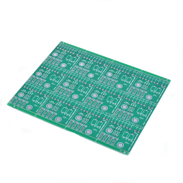
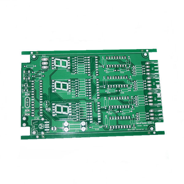
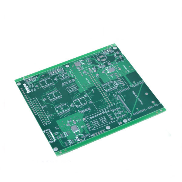
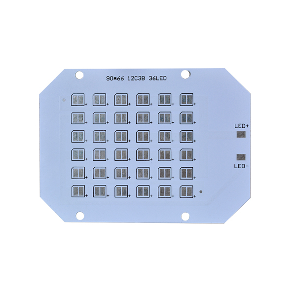
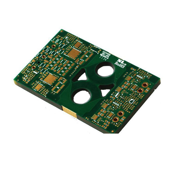
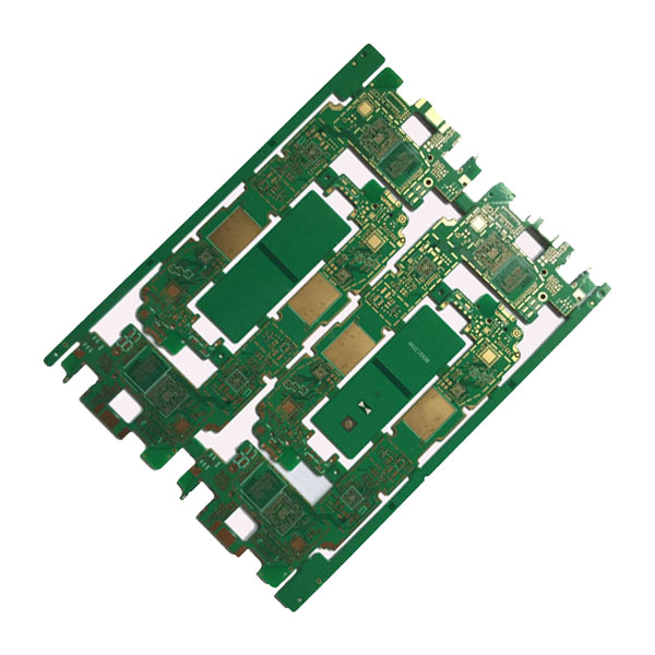
PCB Fabrication
PCB Fabrication is one of our primary services, which is also known as PCB Manufacturing, PCB Printing Service. All our services are under NDA(Non-disclosure Agreement) Protection which makes you stay away from intellectual property concern. Below are the PCB types we manufacture.
Lead Time(Days)
| Single/double side | 4 layer | 6 layer | over 8 layer | HDI | |
| Sample lead time(Normal) | 5-6 | 6-7 | 7-8 | 10-12 | 15-20 |
| Sample lead time(Fastest) | 48-72 hours | 5 | 6 | 6-7 | 12 |
| Mass production lead time(First batch) | 7-9 | 10-12 | 13-15 | 16 | 20 |
PCB Fabrication Capability
| PCB Fabrication Capability | ||
| No | Item | PCB Process Capability |
| 1 | base material | Normal TG FR4, High TG FR4, PTFE, Rogers, Low Dk/Df etc. |
| 2 | Solder mask color | green, red, blue, white, yellow, purple,black |
| 3 | Legend color | white, yellow, black, red |
| 4 | Surface treatment type | ENIG, Immersion tin, HAF, HAF LF, OSP, flash gold, gold finger, sterling silver |
| 5 | Max. layer-up(L) | 50 |
| 6 | Max. unit size (mm) | 620*813 (24″*32″) |
| 7 | Max. working panel size (mm) | 620*900 (24″x35.4″) |
| 8 | Max. board thickness (mm) | 12 |
| 9 | Min. board thickness(mm) | 0.3 |
| 10 | Board thickness tolerance (mm) | T<1.0 mm: +/-0.10mm ; T≥1.00mm: +/-10% |
| 11 | Registration tolerance (mm) | +/-0.10 |
| 12 | Min. mechanical drilling hole diameter (mm) | 0.15 |
| 13 | Min. laser drilling hole diameter(mm) | 0.075 |
| 14 | Max. aspect(through hole) | 15:1 |
| Max. aspect(micro-via) | 1.3:1 | |
| 15 | Min. hole edge to copper space(mm) | L≤10, 0.15;L=12-22,0.175;L=24-34, 0.2;L=36-44, 0.25;L>44, 0.3 |
| 16 | Min. Inner layer clearance(mm) | 0.15 |
| 17 | Min. hole edge to hole edge space(mm) | 0.28 |
| 18 | Min. hole edge to profile line space(mm) | 0.2 |
| 19 | Min. Inner layer copper to profile line space (mm) | 0.2 |
| 20 | Registration tolerance between holes (mm) | ±0.05 |
| 21 | Max. finished copper thickness(um) | Outer Layer: 420 (12oz) Inner Layer: 210 (6oz) |
| 22 | Min. trace width (mm) | 0.075 (3mil) |
| 23 | Min. trace space (mm) | 0.075 (3mil) |
| 24 | Solder mask thickness (um) | line corner: >8 (0.3mil) upon copper: >10 (0.4mil) |
| 25 | ENIG golden thickness (um) | 0.025-0.125 |
| 26 | ENIG nickle thickness (um) | 3-9 |
| 27 | Sterling silver thickness (um) | 0.15-0.75 |
| 28 | Min. HAL tin thickness (um) | 0.75 |
| 29 | Immersion tin thickness (um) | 0.8-1.2 |
| 30 | Hard-thick gold plating gold thickness (um) | 1.27-2.0 |
| 31 | golden finger plating gold thickness (um) | 0.025-1.51 |
| 32 | golden finger plating nickle thickness(um) | 3-15 |
| 33 | flash gold plating gold thickness (um) | 0,025-0.05 |
| 34 | flash gold plating nickle thickness (um) | 3-15 |
| 35 | profile size tolerance (mm) | ±0.08 |
| 36 | Max. solder mask plugging hole size (mm) | 0.7 |
| 37 | BGA pad (mm) | ≥0.25 (HAL or HAL Free:0.35) |
| 38 | V-CUT blade position tolerance (mm) | +/-0.10 |
| 39 | V-CUT position tolerance (mm) | +/-0.10 |
| 40 | Gold finger bevel angle tolerance (o) | +/-5 |
| 41 | Impedance tolerance (%) | +/-5% |
| 42 | Warpage tolerance (%) | 0.75% |
| 43 | Min. legend width (mm) | 0.1 |
| 44 | Fire flame class | 94V-0 |
| Special for Via in pad boards | Resin plugged hole size (min.) (mm) | 0.3 |
| Resin plugged hole size (max.) (mm) | 0.75 | |
| Resin plugged board thickness (min.) (mm) | 0.5 | |
| Resin plugged board thickness (max.) (mm) | 3.5 | |
| Resin plugged maximum aspect ratio | 8:1 | |
| Resin plugged minimum hole to hole space (mm) | 0.4 | |
| different hole size in one board? | yes | |
| Max. panel size (finished) (mm) | 880 ×580 | |
| Max. working panel size (mm) | 914 × 602 | |
| Max. board thickness (mm) | 12 | |
| Max. layer-up(L) | 40 | |
| Aspect | 30:1 (Min. hole: 0.4 mm) | |
| Line wide/space (mm) | 0.075/ 0.075 | |
| Back drill capability | Yes | |
| Tolerance of back drill (mm) | ±0.05 | |
| Tolerance of press fit holes (mm) | ±0.05 | |
| Surface treatment type | OSP, sterling silver, ENIG | |
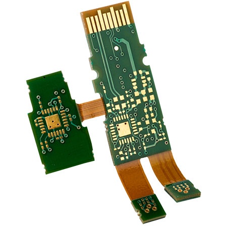
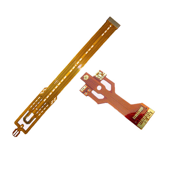
| Rigid-flex board | Hole size (mm) | 0.2 |
| Dielectrical thickness (mm) | 0.025 | |
| Working Panel size (mm) | 350 x 500 | |
| Line wide/space (mm) | 0.075/ 0.075 | |
| Stiffener | Yes | |
| Flex board layers (L) | 8 (4plys of flex board) | |
| Rigid board layers (L) | ≥14 | |
| Surface treatment | All | |
| Flex board in mid or outer layer | Both | |
| Special for HDI products | Laser drilling hole size (mm) | 0.075 |
| Max. dielectric thickness (mm) | 0.15 | |
| Min. dielectric thickness (mm) | 0.05 | |
| Max. aspect | 1.5:1 | |
| Bottom Pad size (under micro-via) (mm) | Hole size+0.15 | |
| Top side Pad size ( on micro-via) (mm) | Hole size+0.15 | |
| Copper filling or not (yes or no) (mm) | yes | |
| Via in Pad design or not ( yes or no) | yes | |
| Buried hole resin plugged (yes or no) | yes | |
| Min. via size can be copper filled (mm) | 0.1 | |
| Max. stack times | 4 | |