
PCB Design
EASTWIN has the complete tools and rich experience to design your PCB. From the schematic built, PCB layout till the electronic products debugging, we will try our best to build the perfect products for each customer. We use the industry’s top-tier design tools and are driven to be the best.
- High speed, multi-layer digital PCB designs – Bus routing, differential pairs, matched lengths.
- HDI Designs with micro vias and advanced materials – Via-in-Pad, laser micro vias.
- PCB Designs for space, military, medical and commercial applications…
- Extensive RF and analog design experience (printed antennas, guard rings, RF shields…)
- Signal integrity issues to meet your digital design needs (tuned traces, diff pairs…)
- PCB Layer management for signal integrity and impedance control
- High-density SMT designs (BGA, uBGA, PCI, PCIE, CPCI…)
- Bluetooth Low Energy Electronic Product design, such as smart wristband, smart home…
- Ultra low EMI designs for MRI applications
- Complete assembly drawings
- In-Circuit Test data generation (ICT)
- Drill, panel and cutout drawings designed
- Professional fabrication documents created
- Autorouting for dense PCB designs
PCB Design Process in Short
![]()
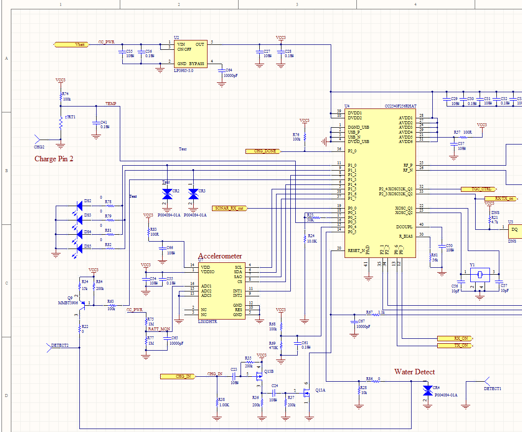
Schematic Diagram Drawing
Before you start drawing wires and stuff, you need to know what circuit you want to build. So you need to find or design schematics for your circuit. And you need a PCB design software. Then you are ready to begin the process.
Start by drawing your schematic diagram into the software you have chosen.
![]()
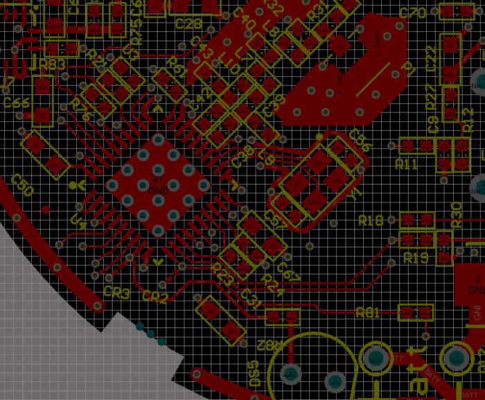
PCB Layout:
Now it’s time to draw the board. We need transfer your schematic diagram into a drawing of your printed circuit board. Most PCB software will have tools that will help you draw your board from the schematic.
![]()
Things To Be Considered During the Design
Will you put the circuit board in a box? Remember that tall components might need to be laid down flat to fit. With a drawing of your components placed on your board, print it out on a sheet of paper. Use this paper version of your board to test that it will fit the box and that your connectors will fit.
![]()
Checking the circuit and Make your PCB manufactured
When you are done drawing your board, it is time to get your PCB design ready for manufacturing.
This basically means you need to check your board for errors and convert your board layout to Gerber files. Then, choose a cheap PCB manufacturer such as Eastwin and get your board fabricated.
EASTWIN PCB design service aims to satisfy customers’ needs as possible as we can. In addition to the PCB hardware design service, we also provide the software design service and even full products design service, please contact us if you are interested in. [email protected]