
- Place of Origin:
-
Guangdong, China (Mainland)
- Brand Name:
-
HT
- Model Number:
-
HT16
- Base Material:
-
FR4/ROGERS/PET/HDI/CEM/PI
- Copper Thickness:
-
0.5-6OZ
- Board Thickness:
-
0.2-7.0mm
- Min. Hole Size:
-
0.15mm
- Min. Line Width:
-
0.075mm/0.1mm(3mil/4mil)
- Min. Line Spacing:
-
3 Mil (0.075 Mm)
- Surface Finishing:
-
ENIG HASL OSP
- Soldermask color:
-
Green,yellow,black,blue,red,white,matte green
- Layer:
-
1-40 ( ≥30 layers needs review )
- silkscreen color:
-
white,black,yellow
- Certificate:
-
UL/ROHS/ISO9001
- SupplyAbility:
- 1000000 Square Meter/Square Meters per Month
- Packaging Details
- usually standard carton/ according to customer
- Port
- Shenzhen/Hongkong
- Lead Time:
- 15 days
Product Description
Hello dear customers,
Welcome to Eastwin Technology.
Eastwin was built up in 1997 to focus on electronic manufacturing solutions service.
Because we always do custom OEM job, there will no clear description of one exact product.
However, we will let you know clearly about our technical capability.
We specialize in:
- PCB design, PCB layout, PCB manufacturing, PCB Assemblies,
- One-stop services from PCB to PCB assembly
- Components sourcing, PCBA Function Test, design solution.
- Electronic testing circuit board or PCBA
- Electronics manufacturing service
Main five types of products we are handling:
- 1) Rigid PCB
- 2) Flexible PCB, and rigid-flex PCB
- 3) Aluminum LED PCB and LED PCBA
- 4) PCBA assembly
- 5) Membrane switch or allkindss of keypads
Technical requirement:
- 1) Professional Surface-mounting and Through-hole soldering Technology
- 2) Various sizes like 1206, 0805,0603 components SMT technology
- 3) ICT(In Circuit Test), FCT (Functional Circuit Test) technology.
- 4) PCB Assembly With UL,CE,FCC,Rohs Approval
- 5) Nitrogen gas reflow soldering technology for SMT.
- 6) High Standard SMT&Solder Assembly Line
- 7) High density interconnected board placement technology capacity.
Know More
PCB Capability
| Eastwin Technology Co., LTD | ||
| Seq | Item | capability |
| 1 | Base Material | FR-4, High TG FR-4 , Halogen Free material ,CEM-3,CEM-1,PTFE,Rogers ,Arlon ,Taconic,Aluminum base,Teflon,PI ,etc |
| 2 | Layers | 1-40 ( ≥30 layers needs review ) |
| 3 | Finished inner/outer copper thickness | 0.5-6OZ |
| 4 | Finished board thickness | 0.2-7.0mm(≤0.2mm needs review),≤0.4mm for HASL |
| Board thickness≤1.0mm: +/-0.1mm 1<Board thickness≤2.0mm: +/-10% Board thickness>2.0mm: +/-8% |
||
| 5 | Max panel size | ≤2sidesPCB: 600*1500mm Multilayer PCB: 500*1200mm |
| 6 | Min conductor line width/spacing | Inner layers: ≥3/3mil Outer layers: ≥3.5/3.5mil |
| 7 | Min hole size | Mechanical hole: 0.15mm Laser hole: 0.1mm |
| Drilling precision: first drilling First drilling: 1mil Second drilling: 4mil |
||
| 8 | Warpage | Board thickness≤0.79mm: β≤1.0% 0.80≤Board thickness≤2.4mm: β≤0.7% Board thickness≥2.5mm: β≤0.5% |
| 9 | Controlled Impedance | +/- 5 % Ω(<50Ω),+/-10%(≥50Ω),≥50Ω+/-5% (needs review) |
| 10 | Aspect Ratio | 15:01 |
| 11 | Min welding ring | 4mil |
| 12 | Min solder mask bridge | ≥0.08mm |
| 13 | Plugging vias capability | 0.2-0.8mm |
| 14 | Hole tolerance | PTH: +/-3mil NPTH: +/-2mil |
| 15 | Outline profile | Rout/ V-cut/ Bridge/ Stamp hole |
| 16 | Solder mask color | Green,yellow,black,blue,red,white,matte green |
| 17 | Component mark color | white,yellow,black |
| 18 | Surface treatment | OSP: 0.2-0.5um HASL: 2-40um Lead free HASL: 2-40um ENIG: Au 1-10U’’ ENEPIG: PB 2-5U’’/ Au 1-8U’’ Immersion Tin:0.8-1.5um Immersion silver: 0.1-1.2um Peelable blue mask Carbon ink Gold plating: Au 1-150U’’ |
| 19 | E-Test | Flying probe tester : 0.4-6.0mm,max 19.6*23.5inch |
| Min spacing from test pad to board edge : 0.5 mm | ||
| Min conductive resistance : 5 Ω | ||
| Max insulation resistance : 250 MΩ | ||
| Max test voltage : 500 V | ||
| Min test pad diameter : 6 mil | ||
| Min test pad to pad spacing: 10 mil | ||
| Max test current : 200 MA | ||
| 20 | AOI | Orbotech SK-75 AOI : 0.05-6.0mm,max 23.5*23.5inch |
| Orbotech Ves machine : 0.05-6.0mm,max 23.5*23.5inch | ||
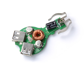
PCBA Assembly
Dear Customer, we offer SMT/DIP/COB/BGA PCB circuits assembly. With 19 years experience, we have built up the strict quality control system.

Packaging & Shipping
Packaging: Standard export carton packing or packing according to the customer’s requirement
Shipping:3-15 days by DHL, UPS, Fedex, TNT, etc.
FAQ
1. What is your minimum order quantity?
A. The MOQ is 1 PCS
2. What payment do you accept?
A. T/T, Western Union, Paypal
3. What kind of PCB file format do I need to submit for production?
A. Gerber files, BOM
4. No PCB file/Gbr file, only have the PCB sample,can you produce it for me?
A. Send us the sample, and we will work out the Gerber files and clone the PCB for you.
5. Are my PCB files safe when I submit them to you for manufacturing?
A:We respect customer’s copyright and will never manufacture PCB for someone else with your files unless we receive written permission from you, nor will we share these files with any other 3rd parties. We can sign NDA with you.
6. How about the lead time?
A:Sample: 5 to 12working days
mass production: 7 to 18 working days
The lead time depends on your final confirmation of the quantity.
7. Which countries have you worked with?
A: We have built cooperation with customers from all over the world, mostly North America and Europe
To give you an exact quote, we hope you could offer us listed information.
1. PCB : Gerber file and other PCB files.
We would appreciate if you can confirm the listed PCB specification also.
1). material 2). board thickness 3). copper thickness 4). surface finishing 5). solder mask color 6). silkscreen color
2. PCBA: PCB files and BOM list
3. If you don’t have ready design files, you can send us a sample, then we will clone for you.
4. We also offer custom PCB design and modify service.
https://www.alibaba.com/product-detail/Car-power-charging-PCBA-assembly-one_60519623675.html