
- Place of Origin:
-
Guangdong, China (Mainland)
- Brand Name:
- Model Number:
-
EW-PCB-circuit board design
- Base Material:
-
FR4
- Copper Thickness:
-
1oz
- Board Thickness:
-
1.6mm
- Min. Hole Size:
-
0.25mm
- Min. Line Width:
-
0.075mm
- Min. Line Spacing:
-
0.075mm
- Surface Finishing:
-
ENIG
- SupplyAbility:
- 1000 Square Meter/Square Meters per Day
- Packaging Details
- Inner packing :Vacuum Package Outer packing:Standard Carton
- Port
- Shenzhen,Hongkong
- Lead Time:
- PCB:5-7 days pcba:20-25 days
Customized PCB Circuit Board Design service
Company Information
Based in Shenzhen, Shenzhen Eastwin Ltd specialize in PCB design, PCB fabrication, components sourcing, and one-stop PCB assembly service, also could provide:
– Reverse Engineering Services
– Fast PCB&PCBA Prototyping
– Cable&Wire Assemblies
– Plastics and Molds
– Function Testing
1.Main Production Equipment (8 SMT LINE 3DIP LINE)
| ITEM | Device Name | Model | Brand Name | Qty | Remarks |
| 1 | Full Automatic Screen Printer | DSP-1008 | DESEN | 8 | |
| 2 | SMT Machine | YG200 | YAMAHA | 5 |
8 SMT Line |
| 3 | SMT Machine | YV100XG | YAMAHA | 3 | |
| 4 | SMT Machine | YG100XGP | YAMAHA | 19 | |
| 5 | SMT Machine | YV88 | YAMAHA | 5 | |
| 6 | Reflow Soldering | 8820SM | NOUSSTAR | 4 | |
| 7 | Reflow Soldering | XPM820 | Vitronics Soltec | 3 | |
| 8 | Reflow Soldering | NS-800 II | JT | 1 | |
| 9 | Solder Paste Inspection | REAL-Z5000 | REAL | 1 | |
| 10 | Automatic Optical Inspection System | B486 | VCTA | 3 | |
| 11 | Automatic Optical Inspection System | HV-736 | HEXI | 5 | |
| 11 | X-Ray | AX8200 | UNICOMP | 1 | |
| 12 | Universal 4*48-pin drive concurrent multiprogramming system | Beehive204 | ELNEC | 3 | |
| 13 | Automatic Plug-In machines | XG-3000 | SCIENCGO | 2 | |
| 14 | Automatic wave soldering system | WS-450 | JT | 1 | 3 DIP LINE |
| 15 | Automatic wave soldering system | MS-450 | JT | 2 |
SMT Assembly LINE

DIP Assembling LINE
Our Services
Product Description
1.Process Capability
1) Bare Printed Circuit Board Process Capability:
| 1 | Layers | Single Sided,2 to 18 Layer |
| 2 | Board material type | FR4, CEM-1, CEM-3, ceramic substrate board, aluminum-based board, high-Tg, Rogers and more |
| 3 | Compound material lamination | 4 to 6 layers |
| 4 | Maximum dimension | 610 x 1,100mm |
| 5 | Dimension tolerance | ±0.13mm |
| 6 | Board thickness coverage | 0.2 to 6.00mm |
| 7 | Board thickness tolerance | ±10% |
| 8 | DK thickness | 0.076 to 6.00mm |
| 9 | Minimum line width | 0.10mm |
| 10 | Minimum line space | 0.10mm |
| 11 | Outer layer copper thickness | 8.75 to 175µm |
| 12 | Inner layer copper thickness | 17.5 to 175µm |
| 13 | Drilling hole diameter (mechanical drill) | 0.25 to 6.00mm |
| 14 | Finished hole diameter (mechanical drill) | 0.20 to 6.00mm |
| 15 | Hole diameter tolerance (mechanical drill) | 0.05mm |
| 16 | Hole position tolerance (mechanical drill) | 0.075mm |
| 17 | Laser drill hole size | 0.10mm |
| 18 | Board thickness and hole diameter ratio | 10:1 |
| 19 | Solder mask type | Green, Yellow, Black, Purple, Blue, White and Red |
| 20 | Minimum solder mask | Ø0.10mm |
| 21 | Minimum size of solder mask separation ring | 0.05mm |
| 22 | Solder mask oil plug hole diameter | 0.25 to 0.60mm |
| 23 | Impedance control tolerance | ±10% |
| 24 | Surface finish | Hot air level, ENIG, immersion silver, gold plating, immersion tin and gold finger |
2) PCBA (PCB Assembly) Process Capability:
| Technical Requirement | Professional Surface-mounting and Through-hole soldering Technology |
| Various sizes like 1206,0805,0603 components SMT technology | |
| ICT(In Circuit Test), FCT(Functional Circuit Test) technology | |
| PCB Assembly With UL,CE,FCC,Rohs Approval | |
| Nitrogen gas reflow soldering technology for SMT | |
| High Standard SMT&Solder Assembly Line | |
| High-density interconnected board placement technology capacity | |
| Quote&Production Requirement | Gerber File or PCB File for Bare PCB Board Fabrication |
| Bom(Bill of Material) for Assembly,PNP(Pick and Place file) and Components Position also needed in assembly | |
| To reduce the quote time, please provide us the full part number for each components, Quantity per board also the quantity for orders. | |
| Testing Guide&Function Testing method to ensure the quality to reach nearly 0% scrap rate | |
| OEM/ODM/EMS Services | PCBA, PCB assembly: SMT & PTH & BGA |
| PCBA and enclosure design | |
| Components sourcing and purchasing | |
| Quick prototyping | |
| Plastic injection molding | |
| Metal sheet stamping | |
| Final assembly | |
| Test: AOI, In-Circuit Test (ICT), Functional Test (FCT) | |
| Customs clearance for material importing and product exporting | |
| Other PCB Assembly Equipments | SMT Machine: SIEMENS SIPLACE D1/D2 / SIEMENS SIPLACE S20/F4 |
| Reflow Oven: FolunGwin FL-RX860 | |
| Wave Soldering Machine: FolunGwin ADS300 | |
| Automated Optical Inspection (AOI): Aleader ALD-H-350B, X-RAY Testing Service | |
| Fully Automatic SMT Stencil Printer: FolunGwin Win-5
|
2.PCBA Production Flow
Eastwin, the Most professional R&D and OEM PCB Assembly Manufacturer in China!
3. PCB&PCBA Certificate
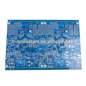
4. PCBA(PCB Assembly) Products Show
Packaging & Shipping
FAQ
Q: What files do you use in bare PCB fabrication?
A:Gerber RS-274X,274D,Eagle and AutoCAD’s DXF,DWG
Q: What format of Bom List you prefer?
A: We prefer in MS-Excel with Components Part No., Manufacturer, Quantity, Value info, other format are also accepted.
Q:How can i know the processing about my PCBA order?
A: Each Customer will have a sale to contact you. Eastwin working hours: AM 9:00-PM 6:00(Beijing Time) from Monday to Friday. we will reply your email in 2hours during our working time. And you also could contact with our sales by cell phone if urgent.
Q: How long will we get the quotation after providing PCB Gerber file, completed bom list, part datasheet and PNP file?
A: The quotation will be sent in less than 2 work days, for some special components, you also could recommend a supplier to us.
Q:If all PCBAs will be tested before delivery if we provide the function testing method?
A: Yes, we ensure that each piece of PCBA will be tested before shipment, we ensure the goods we sent with good quality.
https://www.alibaba.com/product-detail/Customized-PCB-Circuit-Board-Design-service_60042700206.html